2025.05.07 - #34 - NVIDIA/AMD/Google/Furiosa GPU NPU TPU 리뷰, Differentiable rendering 리뷰 #36
Description
NVIDIA GPU, Google TPU, AMD GPU, Furiosa NPU 비교
NVIDIA GPU (A100, H100, H200, B200)
- 공부하기 좋은 리소스: https://comsys-pim.tistory.com/6
Streaming multiprocessors (SM)
- CUDA core (FP32/FP64) + Tensor core (matrix math)
- A100: 108 SMs -> FP64, FP32, FP16, BF16, INT8, INT4 matrix ops
- H100: 132 SMs -> FP64, FP32, FP16, BF16, FP8 (transformer engine)
- 2x tensor FLOPS than A100
- H200: Better memory and power than H100
- B200: 2 x 132 SMs (Dual chiplet, connected by NVLink-C2C) -> FP64, FP32, FP16, BF16, FP8, INT8, INT4, FP4
- 2x tensor FLOPS than H200

Memory
- A100: 40MB L2 cache, HBM2 (40GB @1.6TB/s, 80GB @2.0TB/s)
- H100: 50MB L2 cache, HBM3 (80GB @3.35B/s, [email protected]/s)
- H200: HBM3e (141 GB @4.8TB/s)
- B200: 100MB L2 cache, 8+ HBM3e (192GB @5.3TB/s)

AMD GPU (MI250, MI300)
- GPU based, but pure compute focus
Compute Dies
- MI250X (2021 - CDNA2)
- 2 GPU chiplets - 2 x 110 compute units (Graphics Compute Die - GCD), optimized for FP64 and matrix math
- Matrix cores - FP16, BF16
- MI300 (2023, CDNA3)
- 8 GPU chipets - 304 compute units (Accelerator Complex Dies - XCDs)
- Matrix cores - FP16, BF16, INT8, FP8
- Comparable to H100's raw compute


Memory
- MI250X: 8MB L2 cache per GCD, HBM2e (128GB @3.2TB/s)
- MI300X, 256 'AMD Infinity Cache', HBM3 (192GB @5.3TB/s)
Google TPU (v4, v5e)
- Systolic array core

Processors (TensorCores - large matrix multiply units, SparseCores - Sparse computation)
- TPU v4: 2 TensorCores per chip -> BF16, INT8 (275 TFLOPS per chip for BF16!)
- TPU v5e: 1 TensorCore per chip -> BF16, INT8 (197 TFLOPS for BF16, 393 INT8 TOPS)
- Both uses SparseCores, specialized for embedding vectors, which significantly speed up recommendation and language models with large embedding tables.
- Google uses BF16 for training, and INT8 for inference, and does NOT support FP8 (for v4 and v5e)
Memory
- TPU v4: HBM2 (16GB @1.2 TB/s), Local SRAM 64MB
- TPU v5e: HBM2e (16GB @819 GB/s),
- TPU v5p: HBM3 (95GB @2.8 TB/s)
- TPU v6: HBM3 (192GB @7.4 TB/s)
Architecture
- Scale up:
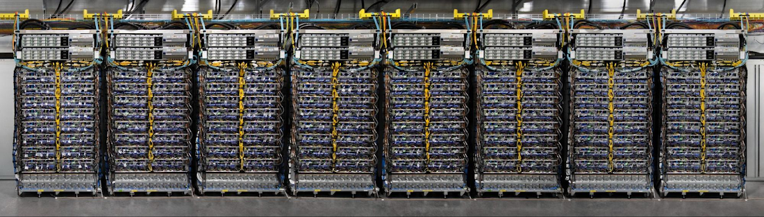
- TPU v4: 4092 chips in a 'pod'
- 아래 이미지는 1개의 'pod' 중의 1/8 이라고 함
- 4x4x4 shape -> 3D torus network
- TPU v5e: 256 chips in a 'pod' for smaller deployment
- TPU v6: 256 chips in a 'pod', or 9216 chips in a 'pod'
- TPU v4: 4092 chips in a 'pod'


Furiosa NPU
Processor (Tensor Contraction Processors - TCP)
- Warboy: 2 TCP cores, FP32, FP16, BF16, FP8, INT8
- 32 TOPS INT8, 4 TFLOPS FP16
- RNGD: 8 TCP cores
- 32 BF16 TFLOPS, 64 TFLOPS FP8 for each core -> 256 TFLOPS BF16, 512 TFLOPS FP8, 1024 TOPS INT4.
Memory
- Warboy: 16GB LPDDR4X (@66GB/s), 32MB on-chip SRAM
- RNGD: 48GB HBM3 (@1.5TB/S), 256 MB on-xhip SRAM
Metadata
Metadata
Assignees
Labels
No labels